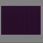
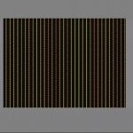
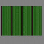
Most of you will be used to the distinctive ‘power on’ screen of the 48K Spectrum, where the screen goes black with a white border, and for a fraction of a second vertical red bars can be seen, before the screen clears to the copyright message.
Those of you who unfortunately have had faulty 48K Spectrums will have seen a different type of pattern that may or may not be close to the standard power on pattern.
Today I’m going to explain what these patterns mean, and if you have a fault, how these can be interpreted to determine with a reasonable level of confidence exactly which memory chip is faulty.
The information in this article relating to the memory test is specific to the 16K/48K Spectrum, 128 machines have a different method of checking RAM which I’ll cover some other time.
Also, I’m assuming that all relevant voltage lines to the lower RAM (+5v, -5v, +12v) have already been checked and verified.
Memory Checking at Power On
When you power on your Spectrum, one of the first things that happens is that the border colour is set to white. For this to happen, the ROM and CPU must be working, so a consistent white border is a good tell-tale sign, if you have a fault, that these parts at least are okay.
The memory check routine then performs the following actions:
- Fills memory from 65535 downwards to 16384 with the value 2
- Starting at address 16384, the following checks are performed:
a) That the value at each address is still 2
b) When the value at that specific address is set to 1, that the value can be read back as 1
c) When the value at that specific address is set to 0, that the value can be read back as 0
When the routine finds an address that fails one of the checks (a), (b) or (c), it stores ( current address-1) as the topmost memory location that can be successfully used. This ends up in the system variable RAMTOP.
So, how does this produce the screen patterning that you see on power on? To understand this, a quick refresher of how the Spectrum handles display bytes is required.
Memory between 16384 and 22527 (0x4000 – 0x57FF) is used for the pixel data, while memory between 22528 and 23295 (0x5800-0x5AFF) holds attribute data.
Attribute data is interpreted by the ULA as follows:

Now back to our test routine. You’ll remember that the value 2 is set to all memory locations, and two in binary is 00000010. Referring to our diagram above, this will produce attributes red ink on black paper, no bright, no flashing. It’ll also produce a single vertical line by way of pixel data.
Since the transition of this value from 2 to 1 does move the pixel position one bit to the right, and change the colour to blue ink/black paper, as this is done a byte at a time the transition to blue usually can’t be seen and the only thing we see is the clearance of the red stripes.
When It All Goes Wrong
So, what happens when you have a faulty lower RAM IC? Let’s take IC10 as an example. Lower RAM IC’s on the 48K spectrum are designated IC6 to IC13, and represent bits 0 to 7 in that order – each memory IC provides a single bit of each byte. So if IC10 is faulty, then bit 4 of any byte in memory will be affected.
When memory IC’s go bad, they typically exhibit one of two behaviours – either they always read back as 1, or their value floats at random. (If you’re truly unlucky they will lock that data line solid, and the CPU won’t be able to execute code.)
Therefore, when the memory test routine runs and tries to store the value of 2 in all memory locations, what’ll actually get read back is, in binary, 00010010. Since the lower RAM IC’s usually fail completely, the attempt by the memory test routine to verify location 16384 will fail, leaving the memory pattern visible with the faults evident in the pattern.
Using our attribute diagram above we can see that this correlates to red paper and red ink. This can either produce a completely red display, or due to the aforementioned ‘floating’ effect, a screen that is predominantly red with rapidly moving horizontal black lines (these are produced when the attribute byte for that line is read and the value of IC10, bit 4, reads back as 0).
Below in the gallery I’ve given example screens that result from a failure of each individual RAM IC from IC6 to IC13 inclusive. If you’re lucky and only have one failed IC, this will usually be enough to pinpoint the problem.
Multiple lower RAM IC failures are a little bit more difficult to diagnose, but observation of the pattern produced and the screen attributes visible should allow you to make an educated guess using the attribute diagram provided above. Observation of the position of pixels within attribute squares, if possible, is also a very good indicator of where faults may lie.
One final caveat – if the machine is a 48K Spectrum, it’s possible that an upper RAM IC has failed in such a way that it is holding its particular data line low or high. In this case, the corresponding lower RAM IC will be unable to assert its value on the data bus when read, and it will look like it has failed. If you remove a lower RAM IC and the pattern does not change, then the corresponding upper RAM IC (positions IC15-IC22 for bits 0-7 in that order) should then be suspected.
Gallery of Failure Types
The below screens are what are typically observed for a single lower memory IC failure.
If you have a different type of pattern that looks non-linear or random, or the machine appears to complete the memory test then hangs or crashes, then it’s likely that upper memory is faulty.
Appendix: Initialisation and Memory Test Routine
The below assembly code details the relevant sections of the 48K ROM that deal with initialisation and memory testing. Non-relevant code has been removed.
; When you power on the machine, the CPU is reset and begins executing code
; from address 0x0000 onwards. These are the first instructions from the ROM
; that get executed.

L0000:  DI                      ; Disable Interrupts.
        XOR     A               ; Signal coming from START.
        LD      DE, 0x0000      ; Set pointer to top of possible physical RAM.
        JP      START-NEW       ; Jump forward to common code at START-NEW.

; START-NEW; this is also called when you execute the NEW command, hence the
; same screen patterning as when you power on - the same memory check is
; occurring.

START-NEW:

        LD      A,$07           ; Select a white border
        OUT     ($FE),A         ; and set it now by writing to a port.

        LD      A,$3F           ; Load the accumulator with last page in ROM.
        LD      I,A             ; Set the I register - this remains constant
                                ; and can't be in the range $40 - $7F as 'snow'
                                ; appears on the screen.

; This is the start of the RAM checking routine.

RAM-CHECK:

        LD      H,D             ; Transfer the top value to the HL register
        LD      L,E             ; pair.

; This section fills the RAM from 0xFFFF to 0x4000 with the value 0x02.

RAM-FILL:

        LD      (HL),$02        ; Load memory with $02 - red ink on black paper.
        DEC     HL              ; Decrement memory address.
        CP      H               ; Have we reached ROM - $3F ?
        JR      NZ, RAM-FILL    ; Back to RAM-FILL if not.

; RAM-READ iterates through each memory location from 0x4000 upwards, decrementing
; the value from 2 to 1, and then 1 to 0, checking it at each step.
RAM-READ:

        AND     A               ; Clear carry - prepare to subtract.
        SBC     HL,DE           ; subtract and add back setting
        ADD     HL,DE           ; carry when back at start.
        INC     HL              ; and increment for next iteration.
        JR      NC, RAM-DONE    ; forward to RAM-DONE if we've got back to
                                ; starting point with no errors.

        DEC     (HL)            ; decrement to 1.
        JR      Z, RAM-DONE     ; forward to RAM-DONE if faulty.

        DEC     (HL)            ; decrement to zero.
        JR      Z, RAM-READ     ; back to RAM-READ if zero flag was set.

; At this point, the HL register contains the first memory location that was found
; faulty.
RAM-DONE:

        DEC     HL              ; step back to last valid location.


