A detailed insight into the development of the ZX Spectrum hardware
Many thanks to Mark Smith who contributed this article and the substantial research effort behind it
So for ages, I’d been intrigued by this:

and this:

At first, I’d looked at them and thought “Ah yes, Issue one board, with ZX81 power connector and funny coloured resistors and capacitors”. But then I looked a bit more closely, and realised that the PCB itself was actually different.
For one thing, just above the heatsink there were two large black electrolytic capacitors, and solder pads specially for them (which are not present on the issue one board), and the other electrolytic capacitors that are usually found dotted around the issue one board were missing.
For another, the tracks near the speaker, and to the left of the board, were different. There were also no silk screen markings on the top, and the board had a uniform beige hue that suggested there was no green solder resist on the underside.
Looking closer still, there were two small tracks missing near the expansion connector, the “ROM” (or what was supposed to be the ROM) was actually inserted upside down, and in the colour publicity photo there were various components missing at various places around the board. Noting that the trimmers were still adjusted to their dead-centre positions, this was clearly a prototype board that had been photographed even before it had been finished being built, and had never been run up and tested for the first time.
Being a bit of an “anorak”, and having built my own PCBs before (e.g. the “SLAM” series of ULA replacement modules), I decided to have a go at making a reproduction of this “issue zero” prototype board.
Step One
The first step was to somehow reproduce the Issue one board, and then I would be able to reverse the changes that were incorporated into it, and arrive at the Issue zero. Peter Smith from ZX Renew very kindly sent me (free of charge!) a partially depopulated issue one board, missing its ULA. I completely stripped the board of all of its components, scanned both sides at high resolution, and then rebuilt it to working condition.
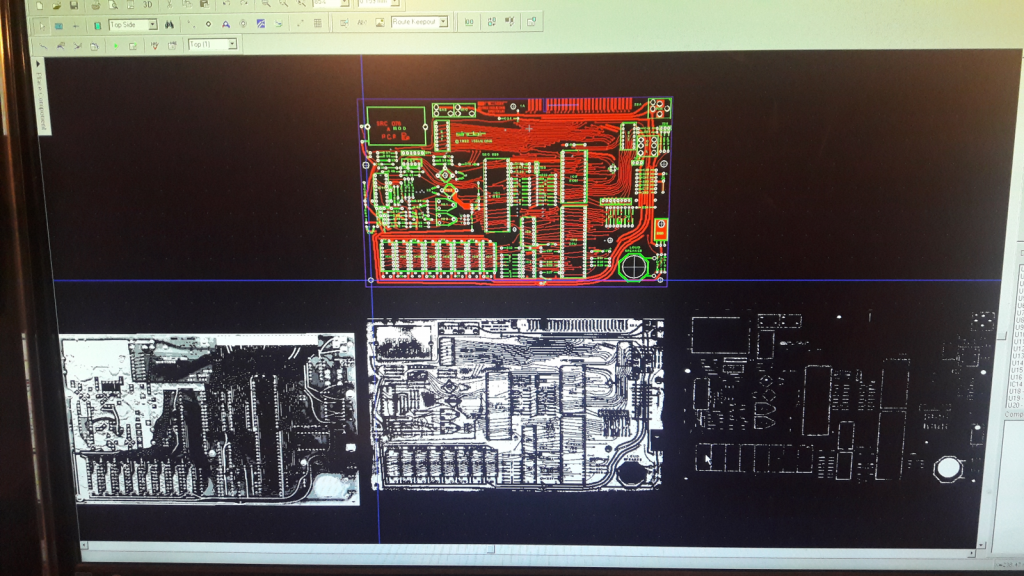
I then downscaled the images of the top and bottom of the board, converted them to monochrome, messed about with mirroring and brightness/contrast, and imported the images into my favourite PCB drawing package. Then started the long task of firstly adding component holes and signal vias, and then drawing curved lines and shapes over the top of the board images to match the original tracks on both top and bottom layers.
Having done that (which took me several months to get round to completing), I also re-drew the silk screen markings, and then I was in the position of being able to create gerber files for PCB manufacture of the issue one board (although due to the rarity and value of those machines, that won’t be happening so don’t ask! 😊).
Step Zero
So then, began the task of undoing the changes that had been made to the prototype board to turn it into the Issue one board. After painstakingly analysing the images for any and all changes, the changes turned out to fall into several different categories, done for various good reasons (as eventually became apparent after I’d built and tested one of the Issue zero boards):
- Improving the TV picture
- Improving resistance to stupid or ”adventurous” users
- Improving reliability of the DC-DC converter
- Fixing circuit design and layout errors
- Tidying up after design decisions had been made
Taking each of these areas in turn:
Improving the TV Picture
On the Issue one board, C44 and C45 are located at lower mid and left-hand positions on the board, whereas on the Issue zero board they are both located above the right-hand keyboard connector. R27 is moved upwards on the Issue one board as a consequence of this.

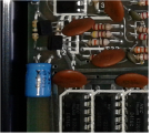

On the Issue one board, the analogue 5V power rail used for the video modulator and TR1/TR2 is isolated from the main 5V rail by R64 and is smoothed by C25, whereas on the Issue zero the 5V rail is common to the whole board. This required changes to the thick power tracks to the left of the LM1889 chip, and rolling those changes back results in a much cleaner layout that quite obviously is what was originally there (confirmed by the photo in the publicity brochure).
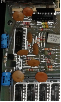
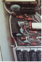
On the Issue one board, C34 is added at the top of the board (smoothing the output of the 5V regulator), and is absent on the Issue zero board. The thick power track that connects to C34’s right-hand leg is extended a bit to reach it on the Issue one board.

Issue one boards also have a 22uF capacitor (C50) added on the power socket itself (smoothing the input to the 5V regulator – it turns out that this is critical to prevent oscillation of the 5V regulator).
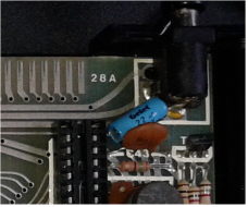
On the issue one board, C47 is located to the right of the speaker (requiring a few changes to the tracking – addition of the horizontal power track under the speaker which looks like an afterthought because it was!), whereas on the Issue zero board it is located under the heatsink, just above R54. In fact, the Issue one board still has component holes for C47 to be able to be located there.
Presumably, the value of C47 used to be less (probably 1uF) and was able to fit under the heatsink, like C27, and during development they decided to increase the value of C47, which meant it was bigger and had to be relocated to near the speaker.
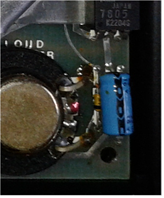
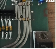
On the Issue one board, C28 is added next to the ULA, to reduce noise on the ULA’s power input and thereby improve the TV picture.
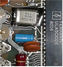
R25 on both boards is fed by 5V for the CPU clock driver TR3. On the Issue one board, R25 is fed by the short right-heading track to a via, which links to an underside track up to the right-hand leg of C34.

On the picture of the “Issue zero” prototype, that track is not there, but instead there is a shadow of a via next to pin 5 of the ULA, which is not there on the issue one board.

It can therefore be deduced that R25 is fed by a track under the ULA to that via, which logically links to the nearest source of power on the underside of the board – the feed to C29/pin 14 of the ULA.
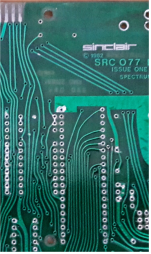
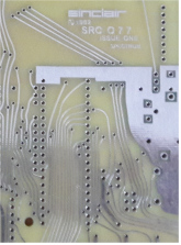
This was likely changed to reduce the amount of interaction between the 3.5MHz CPU clock pulses and the video signal – in other words, it was changed to try to reduce dot crawl.
Incidentally, also visible in this picture of the underside of the Issue one board, is the rather hastily-added thick ground trace coming down the right-hand side of the ULA to connect to newly-added C28.
Improving Resistance to Stupid Users
Near the edge connector, the issue one board has two additional narrow tracks next to the two slanted thick tracks to the left of the right-hand memory expansion socket.

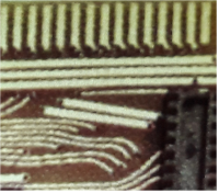
These are to swap the /RESET and /BUSRQ signals with the +12V and +12Vunsmoothed power rails on the edge connector. If the ZX81 edge connector signal positions had been used unmodified on the Spectrum, /RESET would have been at 23A (21A on the ZX81, the 18th position from the slot on the topside), and /BUSRQ would have been on at 22A (20A on the ZX81, the 17th position from the slot on the topside).
On the underside, Stuart Honeyball, while laying out the Spectrum PCB, moved the address lines A8-A15 away from their ZX81 positions which would have been 13B-20B (11B-18B on the ZX81, the 8th-15th positions from the slot on the underside). Presumably this was because it was impossible to route those signals from the Z80, all the way up the middle of the board to the ZX81’s expansion connector positions, so he instead routed them to new additional positions at the ends of the Spectrum’s edge connector (hence the Spectrum’s edge connector is wider).

Having moved A8-A15 out the way, he used up the 8 spare old positions by routing the video signals (Y, U, V, Composite) and GND to five of the old positions (14B-18B), put IORQGE on another (13B), and then (from the alignment of the longer thick slanted tracks to the left of the RH memory expansion connector, and the repositioned vias that connect to each edge connector finger), he put +12V and +12V unsmoothed (carried by those two thick diagonal tracks) on the remaining two spare positions (+12V was at position 20B on the underside, and +12V unsmoothed was at position 19B on the underside).
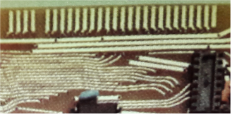
That caused a problem, however. Although the ZX printer doesn’t connect to positions 19B and 20B of the Spectrum’s expansion connector, the ZX81’s 16K RAM pack does, and so any silly user who plugged a Sinclair ZX81 16K ram pack (that they may well have had at home if they were upgrading from a ZX81 to a Spectrum) into their shiny new Spectrum would have found that the Spectrum sent +12V up two of its signal wires, promptly frying the RAM pack, and also probably causing excessive current draw on the Spectrum’s 12V rail, frying TR4 and several 4116 RAMs. Result: dead RAM pack and dead Spectrum, and expensive warranty claim.
Sinclair obviously recognised this, and so redesigned the issue zero board to swap /RESET and /BUSRQ with +12V and +12V smoothed. Neither ZX printer nor ZX81 RAM pack use the ZX81 edge connector’s /RESET or /BUSRQ signals, so by placing +12V and +12V unsmoothed on those positions, no permanent harm would come to either Speccy or ZX81 RAM pack if a silly user tried them together, thus saving Sinclair a lot of money and hassle!
Improving Reliability of the DC-DC Converter
It is evident from the photos that as well as changing the power connector on the production Issue one boards to the usual barrel type, instead of the ZX81-style EAR/MIC type power socket, C43 on the Issue zero board is 47nf rather than the 100nf used on the Issue one.
This probably improved the likelihood that the DC-DC converter would start to oscillate upon power-up (if the oscillator doesn’t start, then TR4 blows), and/or reduced switching noise imparted into the rest of the board from the DC-DC converter circuit.
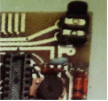
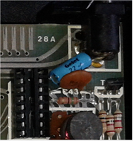
Having run the Issue zero board, I can also report that contact resistance on the ZX81 style power connector can be enough to change the pitch/tone of the whine from the DC-DC converter, so it is conceivable that the barrel style connector increases reliability by reducing problems with bad contacts.
That would have been of no consequence on the ZX81 which only has a 5V regulator inside it, but on the Spectrum with its complicated (and sensitive) DC-DC converter circuit, I can see that there could have been greater problems.
Fixing Circuit Design and Layout Errors
Aside from the lack of power supply smoothing (e.g. missing electrolytic capacitors and R64), the Issue zero suffered from two design/layout errors.
Firstly, the three keyboard pins on the lower right-hand side of the ULA were wired back to front, so that the data lines for keys 3 and 5 (and correspondingly for E and T, D and G, X and V, 6 and 8, Y and I, H and K, B and M) were swapped. This can be seen in the publicity photo, since the tracks to the right of TC1/TC2 are different.
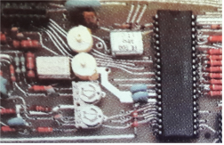

As was the logical thing to do when the layout was made not on a computer, but was done in black tape on acetate film, Stuart re-used some of the existing via holes when fixing the layout – keeping the vias and just changing the tracks that connected to them.
By deduction, it was possible to work out the original track connections and determine that he’d simply got the order of the three keyboard pins on the right-hand side of the ULA wrong (pins 23, 24 & 26). This error can easily be corrected by cutting two tracks on the underside of the Issue zero board, and adding two jumper wires.
It is quite possible that this was not realised to be a problem until the case design was complete, and somebody attempted to design a keyboard membrane with the signals in that order (which is possible, although quite difficult!).
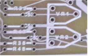
Secondly, the video circuit on the Issue zero differs from the Issue one circuit, specifically in the way that VR1 and VR2 are connected to the U and V outputs from the ULA. On the Issue zero, it’s clear that the upper leg of VR2 and the lower leg of VR1 are connected directly to ground, whereas on the Issue one those legs go via short tracks to unconnected via holes.


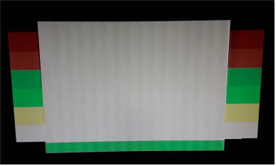
On both boards, the respective wipers of VR1 and VR2 are connected to the U or V signals from the ULA, and the remaining legs of VR1 and VR2 carry a fraction of the U/V signals to the LM1889 chip. On the Issue zero, because one leg of each of VR1 and VR2 is connected to ground, if they are adjusted all the way towards that leg, they short the U or V output from the ULA to ground, killing the ULA.
Regardless, testing proved that even if used with care, this arrangement does not permit proper adjustment of the voltage bias on the Y and V signals, so proper colour adjustment is not possible and the best that can be done results in this:
The fix is to cut off one leg of each of VR1 and VR2, and add R56 and R62 from the respective wipers of VR1 and VR2 to ground (R56 and R62 are missing on the Issue zero, but can be easily added on the back of the board).
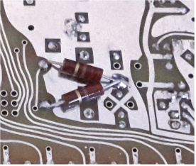
C52 and C53 also have to be moved so that one leg connects to +12V on the Issue one instead of to ground on the Issue zero (for signal smoothing purposes, it doesn’t matter – both are solid fixed voltages).

Tidying Up After Design Decisions Had Been Made
The eagle-eyed will have noticed that the right-hand memory expansion socket on the Issue zero board has 16 pins, whereas the equivalent socket on the issue one board has only 14 pins:
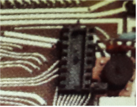

The extra top two pins run very close by to the +12V and the -5V power rails, which are logically the only things that those pins could have been used for, hence that is logically how they should be wired on the Issue zero:


That means that the memory expansion board was initially intended to support 4116 RAMs. And that means that a 32K Spectrum (like its competitor, the BBC model B) was on the cards at some point. Of course, once Sinclair realised that he could buy broken ones of the newly released 64K drams (in which 32K was working) for a similar price to that of 4116 16K DRAMs, the decision was made that the Spectrum would be offered in 16K or 48K versions.
The extra two connector pins then became redundant so they were removed (and also, having now built one of these 16K RAM boards, the extra two pins at the top of the 16pin socket forces the socket to be positioned further forward, and thus the right-hand end of the memory board comes forward by 0.1 inches, which could be enough to stop the memory expansion board fitting properly within the hump at the back of the Spectrum’s case).
Construction and Testing of the Replica Board
A first board (incorrectly supplied by the PCB manufacturer with silk screen markings) was populated with period-style components where possible, fully socketed, and when complete was powered up with only the LM1889 chip and a “stunt” ULA present. (Later on, a second board without silk screen markings was constructed, using all new-old-stock components for authenticity).
A terrible TV picture resulted, absolutely covered in noise and distortion! I checked the +12V and the -5V rails, which were present and correct. There was plenty of noise on the 5V rail, however.
I tried applying the fixes that were made during development to arrive at the Issue one board (adding C50 on the power connector, C34 near the expansion connector, splitting the 5V rail to the video circuit with R64 and adding C25 to smooth it, and adding more smoothing on the 12V rail near the video section – to emulate the way that C45 was moved to the left of the issue one board).
These changes resulted in a much improved picture, although colour remained washed-out:

Notably, none of these changes fixed the display noise on their own, but instead they worked in combination with each other. Thus, the fixes were “clever”, rather than “brute force” (e.g. just bumping up the values of C44 and C45 to some huge and expensive value), and I can imagine that this took some time to work out (perhaps accounting for Sinclair overrunning the promised “28 days from delivery”).
There seemed to be three sources of noise in the TV picture – digital switching noise (the least significant source), switching noise from the DC-DC converter (significant), and oscillation of the 7805 5V linear regulator which was cured by the addition of C50 and C34 (C50 in particular is critical). As mentioned, on the Issue one board the power supply to clock driver TR3 is also re-routed, however I did not bother to “upgrade” that when modifying my prototype “issue zero” board, since it was not possible to modify that easily by hand. I then added the RAM, CPU and address multiplexers, a fully working (non-stunt) ULA, and a ROM:

The machine booted straight up, so I ran a program to create some colour bars, and this was the best I could do (making sure not to adjust VR1 or VR2 all the way and short U or V to ground!)

Having worked out the easiest way to convert the circuit to Issue one spec (cut one leg on VR1 and VR2, and add R56 and R63 on the back), I got the correct colours.
The next problem to fix was the keyboard data line order (two quick snips and the addition of two jumper wires cured that).

Then, to test the board without frying my SMART card or DivMMC, I needed to make a “twister” board to go between the Spectrum and the peripherals, to swap /RESET and /BUSRQ with +12V and +12V unsmoothed. That done, I managed to load some games, and of course found that a 5C102E ULA, without the “dead cockroach” factory modification, gives random key-presses in most machine code games.
However, interestingly, the BiFrost / Nirvana engine games tend to work fine because they synchronise the keyboard reading to the top of the display frame, therefore the ULA data reads for picture generation never clash with keyboard IO port reads.
I then changed the Hitachi ROM for an EPROM. This is easy to do on an Issue zero/one board, since the board has pin 1 of the ROM socket pre-wired to 5V, as required for an EPROM (later board revisions don’t have this because the Spectrum’s ROM doesn’t need it).


The Issue zero/one boards also have a large 5V rail extending down from pin 28 to very close to the four ROM option (Hitachi/NEC) link holes, and all that is needed is to link the top left hole to 5V, and link the lower two holes together. To do a complete job that also gates in MREQ with ROMCS, a ZTX313 (or similar) can easily be added with its collector in the 5V hole, its base in the top right of the four ROM link holes, and its emitter in the bottom right hole.
The existence of R33 makes this scheme possible. No other Spectrum board revision makes the use of an EPROM so easy, and it is very likely that this is because EPROMs were used during development (the mask-programmed production ROMs would only have been ordered at a late stage when the ROM code had been finalised).
I tried the prototype ROM code from the Spectrum prototype at the Centre for Computing History, which worked although due to a bug (it fails to disable interrupts) it often gets stuck in a loop at reset. The standard ROM code works fine, of course.
Finally, I added the 16K “RAM16” expansion board that I also made, to use the extra +12V and -5V power rails on the right-hand memory expansion socket.


I had fun seeing Manic Miner run with only 4 levels, and Ant Attack run with a city made from random data read from non-existent memory at C000-FFFF. The standard ROM code detects the extra ram correctly, and reports P_RAMT at 49151 as expected for only a 16K expansion. The DC-DC converter circuit copes fine with the extra load on +12v and -5V that the 8x additional 4116 rams on the expansion board present.
First Repro ‘Issue Zero’ Machine with 16K Expansion Daughtercard

Second Repro ‘Issue Zero’ machine with new old stock components, as ‘found’ 😊

Further Notes
As noted above, the Issue one board has a legacy footprint for C47 under the heatsink – just above R54. That is the original position of C47, before it was presumably found that it needed to be a larger value that wouldn’t physically fit under the heatsink.

Both boards also have an unmarked location for a capacitor between pin 1 of the 74LS157 RAM address muxes and ground. This is just between the two 74LS157 chips, and could have been used to delay the mux switching if needed.


As it turned out later in production, many Issue one boards were fitted with a small capacitor between /RAS on the 4116 RAMs and ground, to delay /RAS to the RAMs relative to the address lines. So it seems that the opposite problem arose in practice – the address muxes were too slow, rather than too fast, therefore the facility to slow down the address muxes with this extra capacitor footprint between IC3 and IC4 was never used.
The Issue zero board has a large round pad visible by the power connector – I have interpreted this to be one of a line of pads for a different style of 3.5mm jack socket (it does not appear to be compatible with the later barrel type power socket).


The power tracks under R49-R51 in the video section are quite different on the Issue zero – and much cleaner/more logical than the tracks on the Issue one board which look very much like afterthoughts (especially the loop over the thick track that runs under C47, R63, R38 and R48 – that thick track was added on the issue one to connect two parts of the 12V rail).


The addition of R56 and R63 to fix the U and V video circuits very strongly appears to have been hacked into an existing layout – hence, reverting to the previous circuit where VR1 and VR2 are more logically used as simple potential dividers (as a designer would probably expect to use them), cleans up the board layout a lot, with the result that on the Issue zero board there are no components installed at an angle.

The underside of the video section involved a fair bit of logical deduction to arrive at a layout for the issue zero which connected all necessary power rails and grounds in a sensible way, given the changes on the topside which are certainly known.
The beauty of this being a hand-drawn board is that when Stuart Honeyball changed the layout, he invariably left behind traces of the previous layout (e.g. when connections needed to be rewired, via holes were often left in their original locations and only the tracks that connected to them were changed, also the shape of ground plane fills on the underside followed the line of adjacent signal/power traces, and when signal/power traces were moved, the shape of the original traces can still be seen from the outlines of the ground plane fills which were left unchanged in some areas).
Thus, although the underside of this replica board cannot be proven to be completely accurate, logically it is likely to be very similar to what was originally laid out.


As mentioned earlier, “There were also no silk screen markings on the top, and the board had a uniform beige hue that suggested there was no green solder resist on the underside”. This is borne out by the fact that the “SRC” numbers for the top silk screen and bottom solder resist layers on the issue one board are numbered much later than the top and bottom signal layers, suggesting that the top silk and bottom solder mask layers were only created later on when the machines were ready for production, after the “issue zero” had been developed into the production issue one board, and even after the RAM32 expansion board had been prototyped and tested).

Was it worth it? To reverse-engineer the design changes that Altwasser made, and to better understand how the design evolved, and why certain things are the way that they are – definitely!
